Sega Genesis / Mega Drive 1 RGB Bypass
PLEASE READ: THIS PAGE IS AN OVERVIEW AND DOESN’T HAVE INSTRUCTIONS FOR EVERY MOTHERBOARD REVISION. RGB BYPASSING A GENESIS SHOULD BE CONSIDERED AN “EXPERT INSTALLATION” AND YOU’LL MOST LIKELY NEED MORE INFO THAN WHAT’S PROVIDED HERE. I’LL TRY AND UPDATE SOON WITH MORE INFO.
Genesis / Mega Drive 1 consoles do not require a modification for RGB-output, simply a cable. This page is an “experts-only” page that shows how to bypass the Genesis’ internal RGB amp with a different one. All details are below, but this mod requires you to make irreversible modifications to your Genesis system. Beginner and intermediate modders should not try this mod!

Please make sure to read the main Genesis RGB Bypass page before proceeding to make sure that this mod is something you’d really like to try!!! You must read the sections about sync requirements and RGB cables, as it might change the way you approach this mod!!! Also, there are many different revision Genesis / Mega Drive 1’s and each will look different inside. Use these instructions as a basic guide, but you’ll need to double check each detail on your console.
Tools / Parts Needed:
You’ll need a few tools for this mod (more info on the tools can be found in the tools section):
– Genesis Triple Bypass Board or other RGB bypass solution
– Excellent soldering skills.
– Philips head screwdriver
– Soldering iron / solder
– Thin gauge wire
– Small, sharp, cutting tool
– Small pick or x-acto knife if you’re lifting pins
– Solder remover; A de-soldering iron is recommended
– Multimeter
Using a Genesis 2-style Mini DIN / Removing the RF module:
Note: You can skip this if you plan on just using the stock model 1 output DIN. This would be common to skip on Japanese Mega Drive’s that don’t have an RF jack, but is recommended on all other models:
– Start by completely disassembling your console, including removal of the heat sink. Now flip the motherboard over and de-solder the RF adapter. WARNING: If you don’t have a good desoldering gun, this will be a major pain!:

– Place the Genesis 2 style DIN where the RF board used to be and align it with the back of the IO ports. Once it’s perfectly aligned, mark off it’s position on the motherboard:

– Carefully scrape off the green PCB around the area where the new DIN will go. Try and get it as even and “shiny/smooth” as possible (better pic coming soon):
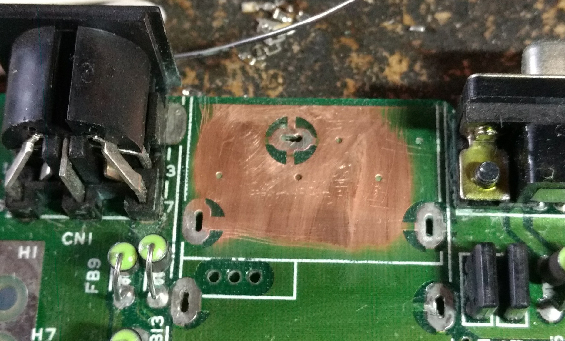
– Use your soldering iron and slightly higher heat than normal to solder the DIN in place. Depending on your needs, you might choose to remove the original DIN as well:

– Now you have a Genesis 2 style output port on a Genesis 1! This will allow for stereo audio through one cable and make 32x connectivity slightly easier! The triple bypass boards will sit right on top of this, or if you’re doing a different installation, you can get a basic breakout board to sit on top of it as well.

Tapping RGBs / Removing “RAM Noise”:
This is the part that you should be most careful of, as these pins can easily break!!! Also, placement of the two capacitors are crucial, otherwise this bypass will actually amplify the interference and “ram noise” on the model 1 motherboards.
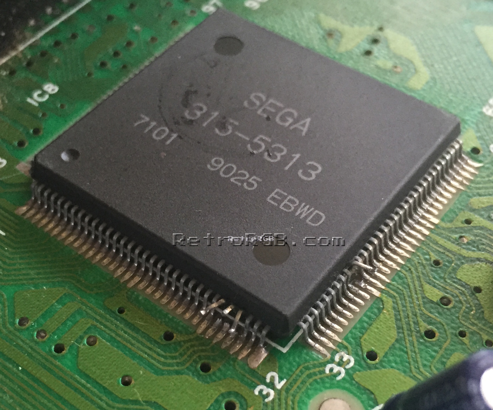
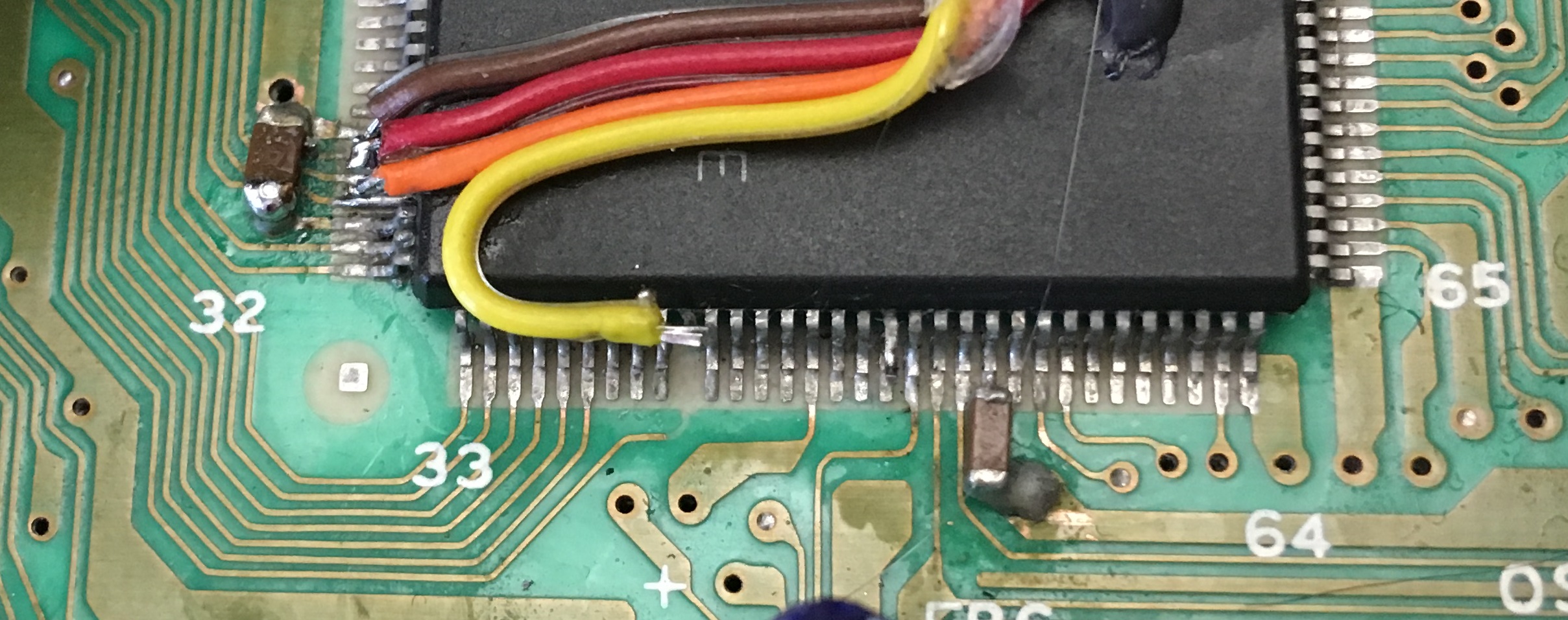
– Locate the VDP. This is a VA3 motherboard with a Sega 315-5313, but the chip may be in a different place (or rotated differently) on your console. Then look up (or trace) which pins are RGB and carefully lft them. Some tips:
– ALWAYS double check which pins are RGB!!! Different VDP’s might have different locations! On the 5313, it’s: Red -> Pin 27 Green -> Pin 28 Blue -> Pin 29
– I chose to only lift RGB. Lifting other pins could potentially cause other issues. I’ll try to replace the pics below soon.
– Don’t remove the stock CXA (or clone encoder).
Click for full-sized picture:
UPDATE!: If you lift the RGB pins, you’ll need to recreate the pullup circuit: https://www.retrorgb.com/fix-for-all-rgb-bypassed-sega-genesis.html
– Next, add a capacitor between the 5v and ground pins that sit next to the RGB pins on the VIA. This should be as close to the via as possible! You’ll need to scrape some of the traces on the motherboard to expose the solder points as well. In my opinion, this is one of the hardest parts of the install.
Here’s the cap we’ve tested with: https://www.arrow.com/en/products/krm31kr71h475kh01l/murata-manufacturing

– Then, add a second capacitor to the output of pin #54 as shown below. Once again that picture shows the sync pin lifted, but it’s not necessary and is probably best to be left down:
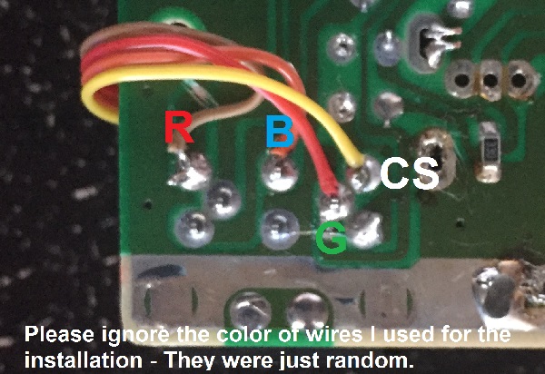
– Now run RGBs to your preferred RGB bypass amp.
If you used a Genesis 2-style DIN, you can connect to that. If you’re only installing a video bypass, you can connect stereo audio via a simple method that taps the headphone amp. Here’s an example of a full triple bypass installation on a VA6 model 1:

Outputting the bypass amp to a Model 1 DIN:
Warning: If you plan on using the original multi-out, cutting is required!
If you decide to use the built-in multi-out, you’ll need to cut the existing traces on the Genesis motherboard, or cut the pins on the CXA chip. It’s my personal opinion that much more can go wrong when cutting traces on the motherboard, which is why I suggest cutting the CXA. You can do whichever you like, but please do so at your own risk!!!
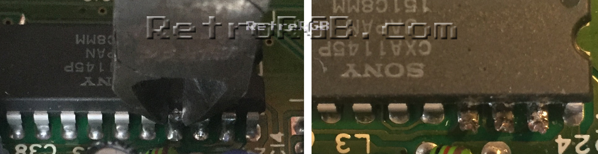
– If you’re soldering to the stock multi-out, start by using a multi-meter to confirm pins 23, 22, 21 & 11 on the Sony CXA1145 connect to RGBs pins 7, 3, 8 & 1 (respectively) on the multi-out. Here’s links and a picture for reference:
http://console5.com/wiki/CXA1145
http://www.gamesx.com/avpinouts/genesisav.htm
This is both to make absolutely sure you’ve located the correct pins on the CXA1145 (the chip will be oriented differently in each version of the motherboard, but the pins are the same) and to make sure there’s no other components between them and the multi-out. For example, if you’re using a Japanese SMS, you might find resistors and capacitors between the CXA1145 and multi-out. In that case, its much safer to simply remove those components, as nothing is “cut” and if you’d ever like to put it back to a stock configuration, simply install new components in their place.
– If there’s no components between the multi-out and the Sony CXA1145, cut and separate pins 23, 22, 21 & 11 from the CXA1145 chip. I found it easiest to cut the top of the pins right where it meets the chip, then use a small flathead to separate them. Only the RGB pins are shown in this close-up picture; The csync (pin 11) is located on the other side of the chip (click for full-sized).
WARNING: Once again, this is most likely irreversible!
– Finally, connect the outputs to the corresponding pins on the multi-out.
– Alternatively, you can solder to the via’s on the motherboard under the CXA. I consider this an expert solution though, as you’d need to be fully aware of what’s going to the DIN and why.
That’s it for now. This page will be updated as soon as more info is available.
If you’re done, please head back to the main Genesis page. If you’d like info on mods for other systems, head to the Getting RGB From Each System page or check out the main page for more retro-awesomeness.